| CPC H01L 23/3675 (2013.01) [H01L 23/13 (2013.01); H01L 23/49816 (2013.01); H01L 23/49827 (2013.01); H01L 23/49838 (2013.01); H01L 24/16 (2013.01); H01L 24/27 (2013.01); H01L 24/32 (2013.01); H01L 24/73 (2013.01); H01L 24/81 (2013.01); H01L 24/83 (2013.01); H01L 24/92 (2013.01); H01L 25/0655 (2013.01); H01L 2224/16227 (2013.01); H01L 2224/32245 (2013.01); H01L 2224/73253 (2013.01); H01L 2224/92225 (2013.01)] | 20 Claims |

|
1. A package structure, comprising:
a semiconductor device; and
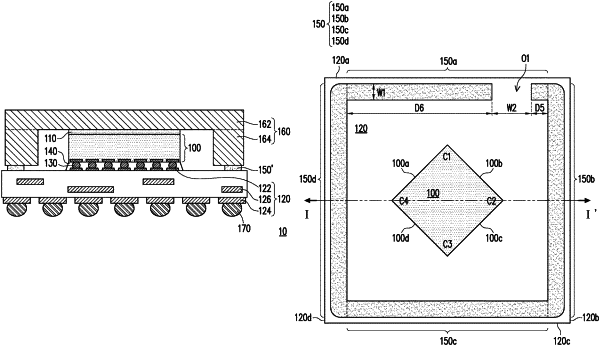
an adhesive pattern, surrounding the semiconductor device, wherein an angle θ is formed between a sidewall of the semiconductor device and a sidewall of the adhesive pattern, 0°<θ<90° wherein the adhesive pattern has a first opening, wherein the first opening is a discontinuous section of the adhesive pattern and connects an inner portion defined by the adhesive pattern and a peripheral portion outside the adhesive pattern, and the first opening is misaligned with a corner of the semiconductor device closest to the first opening.
|