| CPC H01L 23/367 (2013.01) [H01L 23/3157 (2013.01); H01L 23/3738 (2013.01); H01L 23/481 (2013.01); H01L 23/49816 (2013.01); H01L 23/49827 (2013.01); H01L 23/5384 (2013.01)] | 20 Claims |

|
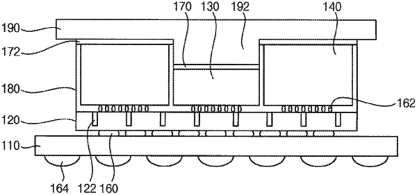
1. A semiconductor package comprising:
a package substrate;
an interposer located over an upper surface of the package substrate and electrically connected with the package substrate;
a logic chip located over an upper surface of the interposer and electrically connected with the interposer;
a memory chip located over the upper surface of the interposer and electrically connected with the interposer and the logic chip, the memory chip having an upper surface that is higher than an upper surface of the logic chip; and
a heat sink including a first lower surface making thermal contact with the upper surface of the memory chip, and a second lower surface extended downwardly from the first lower surface and making thermal contact with the upper surface of the logic chip to dissipate heat in the memory chip and the logic chip,
wherein the first lower surface of the heat sink is positioned over the upper surface of the memory chip.
|