| CPC H01L 23/3192 (2013.01) [H01L 23/3171 (2013.01); H01L 29/66462 (2013.01); H01L 29/7786 (2013.01); H01L 29/7787 (2013.01); H01L 21/0206 (2013.01); H01L 23/291 (2013.01); H01L 29/2003 (2013.01); H01L 29/205 (2013.01)] | 17 Claims |

|
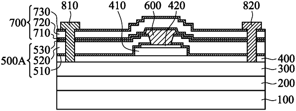
1. A semiconductor structure, comprising:
a substrate;
a channel layer disposed on the substrate;
a barrier layer disposed on the channel layer;
a compound semiconductor layer disposed on the barrier layer and including p-type doped gallium nitride;
a gate electrode disposed on the compound semiconductor layer and having a first side and a second side, wherein the first side and the second side of the gate electrode are parallel to a surface of the substrate,
a stack of dielectric layers conformally disposed on the first side of the gate electrode, wherein the first side of the gate electrode is between the stack of dielectric layers and the gate electrode and the second side of the gate electrode is between the gate electrode and the compound semiconductor layer; and
a dielectric layer covering and exposing a part of the compound semiconductor layer, wherein the stack of dielectric layers covers the dielectric layer,
wherein the stack of dielectric layers comprises at least two layers having different etching rates,
wherein the stack of dielectric layers is in direct contact with the first side of the gate electrode, and the stack of dielectric layers is formed before a source electrode and a drain electrode,
wherein the source electrode is formed as one piece made by a same material extending from a top of the stack of dielectric layers to the barrier layer and in contact with the channel layer; and
wherein the drain electrode is formed as one piece made by a same material extending from the top of the stack of dielectric layers to the barrier layer and in contact with the channel layer.
|