| CPC H01L 22/20 (2013.01) [G01N 21/8806 (2013.01); G01N 21/9503 (2013.01); G01N 2021/8825 (2013.01)] | 7 Claims |

|
1. A method of evaluating a semiconductor wafer, the method comprising:
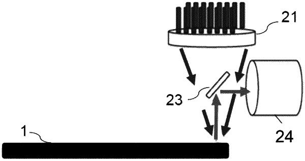
acquiring a reflection image as a bright-field image by receiving reflected light which is obtained when irradiating one surface side of a semiconductor wafer to be evaluated with light;
acquiring a scattered image as a dark-field image by receiving scattered light which is obtained when irradiating the surface side of the semiconductor wafer to be evaluated with light; and
obtaining a distance L between a bright zone that is observed in the reflection image and a bright zone that is observed in the scattered image,
wherein the semiconductor wafer to be evaluated is a semiconductor wafer in which a chamfered surface is formed in a wafer outer peripheral edge section, and
the method further comprising:
evaluating, based on L, a shape of a boundary part between a main surface on the surface side irradiated with the light of the semiconductor wafer to be evaluated and a chamfered surface adjacent to the main surface, and
acquiring the scattered image by irradiating a portion that includes at least a region on a side of the boundary part of the chamfered surface and a region on a side of the chamfered surface of the boundary part with light from a direction ranging from a 10° outside direction to a 50° outside direction, relative to upward in a vertical direction of the boundary part as a 0° direction and a wafer radial direction which is perpendicular to the 0° direction and which passes through the boundary part as a 90° direction.
|