| CPC H01L 22/12 (2013.01) [H01L 21/31144 (2013.01)] | 10 Claims |

|
1. A method of fabricating a semiconductor device, the method comprising:
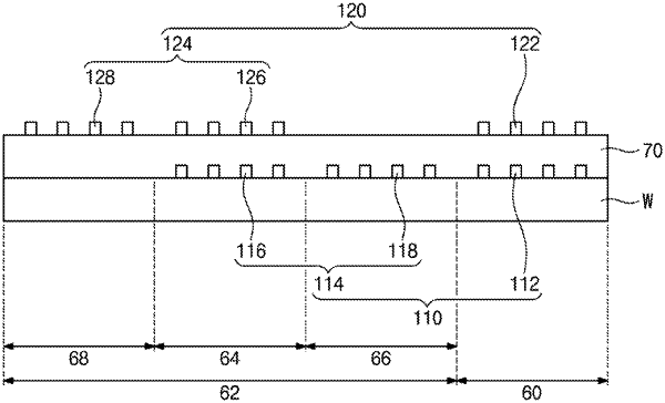
forming a lower pattern on a substrate, the lower pattern including a parent pattern;
forming an upper thin film on the lower pattern and the substrate;
forming a photoresist pattern on the upper thin film, the photoresist pattern including a child pattern located on the parent pattern;
measuring a diffraction light from the parent and child patterns to obtain an intensity difference curve of the diffraction light versus its wavelength;
measuring a first reflection light from the parent pattern to obtain a first reflectance versus its wavelength;
measuring a second reflection light from the child pattern to obtain a second reflectance versus its wavelength;
examining whether a first peak of the first reflectance is smaller than a second peak of the second reflectance; and
obtaining a first wavelength corresponding to a peak of the intensity difference curve located near the first peak, and performing an overlay measurement process on the parent and child patterns using a diffraction light that has the first wavelength to obtain an overlay measurement value, when the first peak is smaller than the second peak.
|