| CPC H01L 22/12 (2013.01) [G01N 21/8851 (2013.01); G01N 21/9501 (2013.01); G01N 21/956 (2013.01)] | 10 Claims |

|
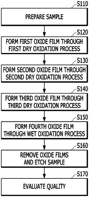
1. A wafer defect region evaluation method comprising:
preparing a sample wafer;
forming a first oxide film on the sample wafer at a temperature of 700° C. to 800° C.;
forming a second oxide film on the first oxide film at a temperature of 800° C. to 1000° C.;
forming a third oxide film on the second oxide film at a temperature of 1000° C. to 1100° C.;
forming a fourth oxide film on the third oxide film at a temperature of 1100° C. to 1200° C.;
removing the first to fourth oxide films;
etching the sample wafer, from which the first to fourth oxide films are removed, to form haze on a surface of the sample wafer; and
evaluating a defect region of the sample wafer based on the haze.
|