| CPC H01L 21/8221 (2013.01) [H01L 21/761 (2013.01); H01L 21/823807 (2013.01); H01L 21/823814 (2013.01); H01L 21/823828 (2013.01); H01L 21/823878 (2013.01); H01L 27/0688 (2013.01); H01L 27/0922 (2013.01); H01L 27/1207 (2013.01); H01L 29/0673 (2013.01); H01L 29/42392 (2013.01); H01L 29/66439 (2013.01); H01L 29/66545 (2013.01); H01L 29/66787 (2013.01); H01L 29/7848 (2013.01)] | 20 Claims |

|
1. A method comprising:
forming a fin structure over a substrate, wherein the fin structure comprises a first channel layer, a sacrificial layer over the first channel layer, and a second channel layer over the sacrificial layer;
forming a dummy gate structure across the fin structure;
recessing the fin structure by using the dummy gate structure as an etch mask;
after recessing the fin structure, epitaxially growing first source/drain epitaxial structures on opposite sides of the first channel layer;
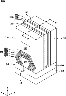
epitaxially growing epitaxial isolation structures on and in contact with the first source/drain epitaxial structures, respectively, wherein epitaxially growing the epitaxial isolation structures comprises:
epitaxially growing a first epitaxial layer on and in contact with one of the first source/drain epitaxial structures;
epitaxially growing a second epitaxial layer on and in contact with the first epitaxial layer;
epitaxially growing a third epitaxial layer on and in contact with the second epitaxial layer; and
epitaxially growing a fourth epitaxial layer on and in contact with the third epitaxial layer, wherein the first and third epitaxial layers are of a first conductivity type, and the second and fourth epitaxial layers are of a second conductivity type different from the first conductivity type;
epitaxially growing second source/drain epitaxial structures on opposite sides of the second channel layer, wherein the second source/drain epitaxial structures are on and in contact with the epitaxial isolation structures, respectively;
removing the dummy gate structure and the sacrificial layer to form a gate trench between the first source/drain epitaxial structures and between the second source/drain epitaxial structures; and
forming a metal gate structure in the gate trench.
|