| CPC H01L 21/76885 (2013.01) [H01L 21/67167 (2013.01); H01L 21/67207 (2013.01); H01L 21/76829 (2013.01); H01L 21/76883 (2013.01); H01L 21/68707 (2013.01)] | 18 Claims |

|
1. A method comprising:
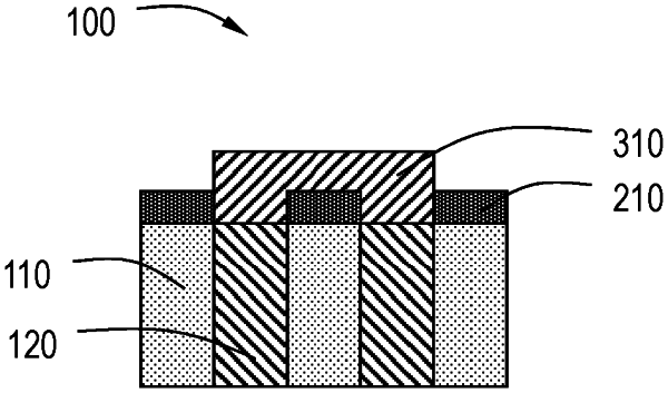
selectively depositing an etch stop layer on a first dielectric material over a first metal material, the first dielectric material comprising a plurality of features formed therein with the first metal material within the plurality of features;
depositing a second metal material on the first metal material and the etch stop layer;
etching the second metal material to expose a portion of the etch stop layer; and
removing the portion of the etch stop layer exposed by etching the second metal material to expose a top surface of the first dielectric material,
wherein a top surface of the second metal material is higher than the exposed top surface of the first dielectric material.
|