| CPC H01L 21/76816 (2013.01) [H01L 21/0273 (2013.01); H01L 21/31111 (2013.01); H01L 21/31144 (2013.01); H01L 21/76825 (2013.01); H01L 21/76877 (2013.01); H01L 21/76897 (2013.01)] | 21 Claims |

|
1. A method of fabricating an interconnect structure for an integrated circuit, the method comprising:
forming a hardmask layer above an inter-layer dielectric (ILD) layer formed above a substrate;
forming a plurality of dielectric spacers on the hardmask layer;
patterning the hardmask layer to form a plurality of first hardmask portions;
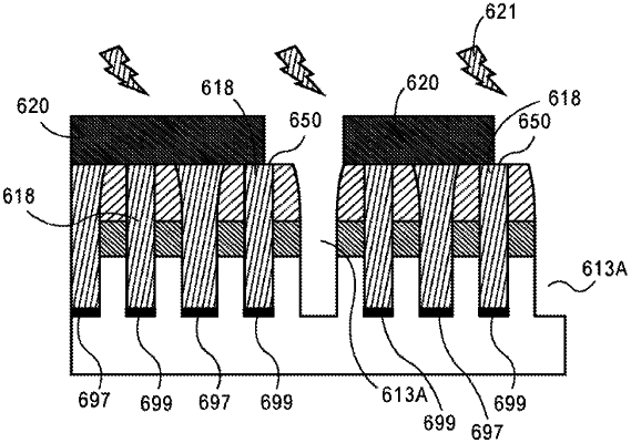
forming a plurality of second hardmask portions alternating with the first hardmask portions, wherein the plurality of second hardmask portions are formed by first forming pore-filled hardmask portions comprising a porous dielectric material filled with metal-containing material, and subsequently removing the metal-containing material;
forming a plurality of electrobuckets on the alternating first and second hardmask portions and in openings between the plurality of dielectric spacers, wherein electrobuckets formed on the first hardmask portions have a different sensitivity to e-beam or extreme ultra-violet (EUV) radiation than electrobuckets formed on the second hardmask portions; and
exposing and removing select ones of the plurality of electrobuckets to a lithographic exposure to define a set of via locations.
|