| CPC H01L 21/477 (2013.01) [H01L 21/3105 (2013.01); H01L 23/562 (2013.01); H10B 41/27 (2023.02); H10B 43/27 (2023.02)] | 9 Claims |

|
1. A method of controlling bow of a substrate, comprising:
providing a substrates;
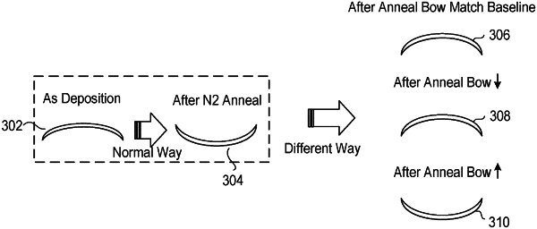
depositing a dielectric layer which includes one of high density plasma (HDP) silicon oxide material and tetraethyl orthosilicate (TEOS) material over the substrate, the substrate having a downward bow with respect to a reference plane and a value of the bow being negative after the one of the HDP silicon oxide material and the TEOS material is deposited on the substrate; and
adjusting the bow of the substrate by performing an annealing process on the substrate, wherein:
the annealing process includes one of a first process condition and a second process condition, the first process condition inducing a tensile stress on the substrate to cause the substrate to bow upward with respect to the reference plane, and the second process condition inducing a compressive stress on the substrate to cause the substrate to bow downward with respect to the reference plane.
|