| CPC H01L 21/0276 (2013.01) [G03F 7/162 (2013.01); G03F 7/168 (2013.01); H01L 21/32139 (2013.01); H01L 21/76802 (2013.01); H01L 21/823842 (2013.01); H01L 21/0332 (2013.01); H01L 21/31138 (2013.01)] | 20 Claims |

|
1. A method of manufacturing a semiconductor device, comprising:
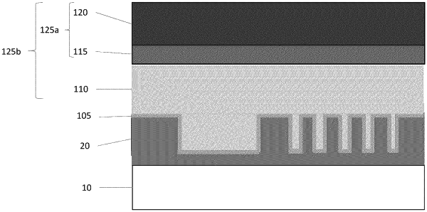
forming a conductive layer over a substrate having a plurality of protrusions and recesses,
wherein the conductive layer is formed over the protrusions and in the recesses;
forming a protective layer over the conductive layer,
wherein the protective layer includes a polymer composition including a polymer comprising repeating units of one or more of:
 wherein a, b, c, d, e, f, g, h, and i are each independently H, —OH, —ROH, —R(OH)2, —NH2, —NHR, —NR2, —SH, —RSH, or —R(SH)2, wherein at least one of a, b, c, d, e, f, g, h, and i on each repeating unit is not H,
wherein R, R1, and R2 are each independently a C1-C10 alkyl group, a C3-C10 cycloalkyl group, a C1-C10 hydroxyalkyl group, a C2-C10 alkoxy group, a C2-C10 alkoxy alkyl group, a C2-C10 acetyl group, a C3-C10 acetylalkyl group, a C1-C10 carboxyl group, a C2-C10 alkyl carboxyl group, or a C4-C10 cycloalkyl carboxyl group, and
n is 2-1000;
forming a resist layer over the protective layer;
patterning the resist layer; and
forming a conductive contact over the conductive layer.
|
|
8. A method of manufacturing a semiconductor device, comprising:
forming a polymer layer over plurality of features disposed over a substrate, wherein the plurality of features are separated by a distance D1 of less than 20 nm and two adjacent features are separated by a gap having a depth D2 from a top surface of the features of greater than 10 nm,
wherein the plurality of features include a metal layer disposed over a plurality of projections extending from a substrate, and
wherein the polymer layer fills the gaps and extends over the top surface of the features;
forming a photoresist layer over the polymer layer;
selectively exposing the photoresist layer to actinic radiation;
developing the selectively exposed photoresist layer to form a photoresist pattern; and
forming a conductive contact in contact with the metal layer after developing the selectively exposed photoresist layer.
|
|
13. A method of manufacturing a semiconductor device, comprising:
forming a conductive layer over a substrate having a topography including a plurality of spaced-apart protrusions having upper surfaces,
wherein a first protrusion and a second protrusion are separated by a distance ranging from 5 nm to less than 20 nm, and a depth of a gap between the first protrusion and the second protrusion from the upper surfaces ranges from 10 nm to 300 nm;
forming a spin on carbon layer comprising a spin on carbon composition over the conductive layer,
wherein the spin on carbon composition comprises a polymer including repeating units including functional groups selected from one or more of —OH, —ROH, —R(OH)2, —NH2, —NHR, —NR2, —SH, —RSH, or —R(SH)2, wherein R is a C1-C10 alkyl group, a C3-C10 cycloalkyl group, a C1-C10 hydroxyalkyl group, a C2-C10 alkoxy group, a C2-C10 alkoxy alkyl group, a C2-C10 acetyl group, a C3-C10 acetylalkyl group, a C1-C10 carboxyl group, a C2-C10 alkyl carboxyl group, or a C4-C10 cycloalkyl carboxyl group;
forming a photoresist layer over the spin on carbon layer;
patternwise imaging the photoresist layer;
developing the photoresist layer to form a pattern in the photoresist layer; and
forming a conductive contact over the conductive layer after developing the photoresist layer.
|