| CPC H01L 21/0217 (2013.01) [C23C 16/00 (2013.01); H01L 21/02208 (2013.01); H01L 21/0228 (2013.01); H01L 21/67703 (2013.01); H01L 21/68771 (2013.01)] | 18 Claims |

|
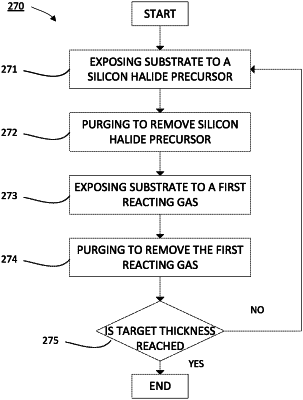
1. A method for forming a silicon nitride film on a substrate in a deposition chamber, wherein the substrate is sequentially exposed to a sequence of processing gases, comprising:
(a) a silicon halide precursor, wherein the silicon halide absorbs onto a surface of the substrate to form an absorbed layer of the silicon halide, and wherein the silicon halide precursor comprises SiHYX4-Y, wherein Y is one of 1, 3 or 4, and wherein X is Cl;
(b) an inert purge gas comprising a gas selected from the group consisting nitrogen gas, argon gas and helium gas;
(c) a first reacting gas comprising N2 and one or both of Ar and He, wherein the first reacting gas is activated using a plasma source; and
(d) a second reacting gas comprising a hydrogen-containing gas and N2, wherein the hydrogen-containing gas includes HN3 (hydrogen azide), wherein the substrate is sequentially exposed to the first reacting gas and then to the second reacting gas without being exposed to an intervening reacting gas; and
repeating the sequence (a) to (d) until a desired thickness of the silicon nitride film is obtained.
|