| CPC H01J 37/32357 (2013.01) [C23C 16/402 (2013.01); G03F 7/427 (2013.01); H01J 37/32724 (2013.01); H01J 37/32733 (2013.01); H01J 37/32899 (2013.01); H01J 2237/338 (2013.01)] | 20 Claims |

|
1. A method for processing substrates, the method comprising:
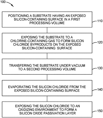
positioning a passivation substrate in a processing volume of a processing chamber, wherein the passivation substrate has a silicon chloride residue formed thereon;
evaporating the silicon chloride residue from the passivation substrate;
depositing the evaporated silicon chloride on one or more interior surfaces in the processing volume;
exposing the deposited silicon chloride to an oxidizing environment to convert the deposited silicon chloride to a silicon oxide passivation layer; and
ashing a layer from a production substrate in the processing volume of the processing chamber having the silicon oxide passivation layer on the one or more interior surfaces.
|