| CPC H01G 9/2045 (2013.01) [H10K 30/10 (2023.02); H10K 71/12 (2023.02)] | 15 Claims |

|
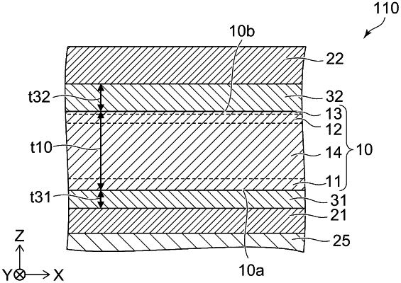
1. A photoelectric conversion element, comprising:
a first conductive layer;
a second conductive layer; and
a photoelectric conversion layer located between the first conductive layer and the second conductive layer,
the photoelectric conversion layer including Sn and Pb,
the photoelectric conversion layer including
a first partial region,
a second partial region between the first partial region and the second conductive layer, and
a third partial region between the second partial region and the second conductive layer,
the first partial region including a first Sn concentration and a first Pb concentration,
the second partial region including at least one of a second Sn concentration or a second Pb concentration,
the second Sn concentration being less than the first Sn concentration,
the second Pb concentration being greater than the first Pb concentration,
the third partial region including Sn, oxygen, and Pb.
|