| CPC H01G 4/30 (2013.01) [H01G 4/008 (2013.01); H01G 4/012 (2013.01); H01G 4/12 (2013.01); H01G 4/232 (2013.01); H01G 4/248 (2013.01)] | 24 Claims |

|
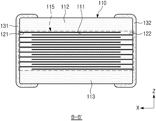
1. A multilayer capacitor comprising:
a body including a stack structure in which at least one first internal electrode and at least one second internal electrode are alternately stacked in a first direction with at least one dielectric layer interposed therebetween thereby defining a capacitance formation region; and
first and second external electrodes spaced apart from each other and disposed on the body to be respectively connected to the at least one first internal electrode and the at least one second internal electrode,
wherein each of the first and second external electrodes includes:
a first conductive layer including a first conductive material and glass; and
an oxide layer including an oxide and disposed on at least a portion of an external surface of the first conductive layer which overlaps the body in the first direction, and
wherein the oxide layer is not disposed on at least a portion of an area of the external surface of the first conductive layer which overlaps the capacitance formation region in a direction in which the first and second external electrodes face each other.
|