| CPC H01G 4/30 (2013.01) [H01G 4/005 (2013.01); H01G 4/06 (2013.01); H01L 23/52 (2013.01); H01L 23/522 (2013.01); H01L 23/535 (2013.01); Y10T 29/43 (2015.01)] | 10 Claims |

|
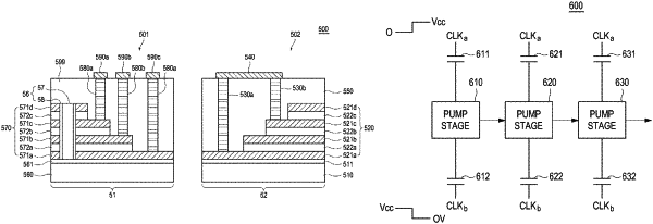
1. A method of forming a memory structure, comprising:
forming a three-dimensional (3D) memory cell region; and
forming a peripheral region adjacent to the memory cell region, including forming a capacitor structure including multiple conductive levels separated by dielectric levels, comprising:
forming a first conductive level, a second conductive level above the first conductive level, and a third conductive level above the second conductive level;
wherein the second conductive level is stepped back from an upper surface end portion of the first conductive level, and wherein the third conductive level is stepped back from an upper surface end portion of the second conductive level;
wherein the first and second conductive levels are separated by a first dielectric level, and wherein the second and third conductive levels are separated by a second dielectric level.
|