| CPC H01B 11/1808 (2013.01) [H01B 3/30 (2013.01); H01B 7/17 (2013.01); H01B 11/1834 (2013.01)] | 6 Claims |

|
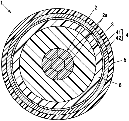
1. A signal transmission cable, comprising:
a conductor;
an insulator covering around the conductor;
a shield layer covering around the insulator;
a sheath covering around the shield layer; and
a plating base layer is provided between the insulator and the shield layer to cover around the insulator,
wherein the shield layer comprises a plating layer provided to cover the plating base layer to be in contact with an outer peripheral surface of the plating base layer,
wherein a surface roughness of an outer peripheral surface of the plating layer is less than a surface roughness of an inner peripheral surface of the plating layer,
the outer peripheral surface of the plating base layer is roughened to have a surface roughness of 2 μm or more, and
the arithmetic mean roughness Ra of the inner peripheral surface of the plating layer is 2 μm or more and the arithmetic mean roughness Ra of the outer peripheral surface of the plating layer is less than 2 μm, and
wherein a thickness of the plating layer is 2 μm or more and 5 μm or less.
|