US 11,955,251 B2
Crystal and substrate of conductive GaAs, and method for forming the same
Takashi Sakurada, Itami (JP); and Tomohiro Kawase, Itami (JP)
Assigned to Sumitomo Electric Industries, Ltd., Osaka (JP)
Filed by SUMITOMO ELECTRIC INDUSTRIES, LTD., Osaka (JP)
Filed on Apr. 19, 2021, as Appl. No. 17/233,845.
Application 15/976,184 is a division of application No. 13/953,421, filed on Jul. 29, 2013, abandoned.
Application 17/233,845 is a continuation of application No. 15/976,184, filed on May 10, 2018, granted, now 11,017,913.
Application 13/953,421 is a continuation of application No. 13/145,145, abandoned, previously published as PCT/JP2010/050628, filed on Jan. 20, 2010.
Claims priority of application No. 2009-010222 (JP), filed on Jan. 20, 2009.
Prior Publication US 2021/0241934 A1, Aug. 5, 2021
Int. Cl. C30B 29/42 (2006.01); C22F 1/16 (2006.01); C30B 11/00 (2006.01); C30B 33/00 (2006.01); C30B 33/02 (2006.01); H01B 1/02 (2006.01)
CPC H01B 1/02 (2013.01) [C22F 1/16 (2013.01); C30B 11/00 (2013.01); C30B 29/42 (2013.01); C30B 33/00 (2013.01); C30B 33/02 (2013.01); Y10T 428/24355 (2015.01)] 13 Claims
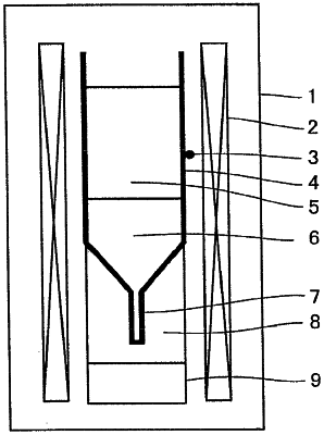
OG exemplary drawing
 
1. A conductive GaAs single crystal substrate cut from a conductive GaAs single crystal, comprising:
a polished mirror surface;
an atomic concentration of Si being more than 1×1017 cm−3; and
a density of precipitates having sizes of at least 30 nm being at most 400 cm−2; wherein
on the polished mirror surface a density of microscopic defects having sizes of at least 0.265 μm measured by a surface particle inspection device is at most 0.3 cm−2, and
an average dislocation density of the substrate is at most 92 cm−2, and
dopants contained in the substrate consist of Si.