| CPC G11C 7/1051 (2013.01) [G11C 7/1006 (2013.01); G11C 7/12 (2013.01); G11C 7/18 (2013.01); G11C 8/08 (2013.01); G11C 8/14 (2013.01)] | 20 Claims |

|
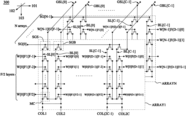
1. A memory device, comprising:
a plurality of arrays coupled in parallel with each other, wherein a first array of the plurality of arrays comprises:
a first switch and a plurality of first memory cells that are arranged in a first column;
a second switch and a plurality of second memory cells that are arranged in a second column; and
first and second data lines that are coupled to the plurality of first memory cells and the plurality of second memory cells,
wherein the second switch is configured to output a data signal from the second data line to a sense amplifier,
wherein control terminals of the first switch and the second switch are coupled together to a control line
wherein first portions of the first and second data lines extend in a row direction below the first and second switches, and
the plurality of first and second memory cells are arranged between the first portions of the first and second data lines and the first to second switches.
|