| CPC G11C 7/1039 (2013.01) [G11C 7/1063 (2013.01); G11C 7/1069 (2013.01); G11C 7/109 (2013.01); G11C 7/1096 (2013.01)] | 15 Claims |

|
1. A memory device, comprising:
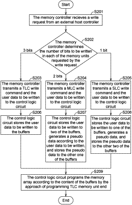
a memory controller, configured to receive a write request and a first data from a host controller, and transmit a write command indicating a first parameter, wherein the first parameter represents the number of bits of binary data to be written into one memory unit; and
a memory, coupled to the memory controller, comprising:
a memory array, comprising a plurality of memory units, each of the memory units configured to store at most N bits of binary data, wherein N is an integer greater than 1;
at least one buffer; and
a control logic circuit, coupled to the memory array and the at least one of buffer, and configured to perform:
in response to the write command, when the first parameter is K which is an positive integer smaller than N, configuring the first data as sub-data every K bit(s), generating a (N−K)-bit pseudo data corresponding to each of the sub-data, and storing the sub-data and the pseudo data into the at least one buffer; and
for each of the memory units to be programmed, programing the memory unit according to the K-bit sub-data to be written into the memory unit and the (N−K)-bit pseudo data corresponding to the sub-data to be written into the memory unit, to cause a threshold voltage of the memory unit to fall within one of 2K voltage ranges selected from 2N voltage ranges, wherein the 2N voltage ranges one-to-one corresponding to 2N data patterns formed by N bits of binary data.
|