| CPC G11C 16/0433 (2013.01) [G11C 5/063 (2013.01); G11C 7/18 (2013.01); G11C 16/08 (2013.01); G11C 16/24 (2013.01); G11C 16/26 (2013.01)] | 20 Claims |

|
1. A nonvolatile semiconductor storage device comprising:
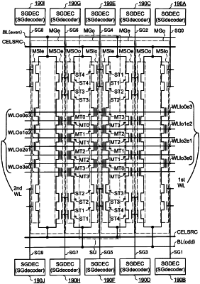
first and second semiconductor layers that extend in a first direction and are spaced apart from each other in a second direction that intersects the first direction, the first semiconductor layer having a first side that is on a side of the second semiconductor layer in the second direction and a second side that is on an opposite side of the first side of the first semiconductor layer, and the second semiconductor layer having a first side that is on a side of the first semiconductor layer in the second direction and a second side that is on an opposite side of the first side of the second semiconductor layer;
first and second bit lines extending in the second direction;
first and second source lines extending in a third direction that intersects the first and second directions and on opposite sides of the first and second semiconductor layers in the first direction;
a first memory string on the first side of the first semiconductor layer and including a first select transistor connected to the first bit line, a second select transistor connected to the first source line, a plurality of first memory cell transistors connected between the first select transistor and the second select transistor;
a second memory string on the second side of the first semiconductor layer and including a third select transistor connected to the first bit line, a fourth select transistor connected to the first source line, and a plurality of second memory cell transistors connected between the third select transistor and the fourth select transistor;
a third memory string on the first side of the second semiconductor layer and including a fifth select transistor connected to the second bit line, a sixth select transistor connected to the second source line, and a plurality of third memory cell transistors connected between the fifth select transistor and the sixth select transistor;
a fourth memory string on the second side of the second semiconductor layer and including a seventh select transistor connected to the second bit line, an eighth select transistor connected to the second source line, and a plurality of fourth memory cell transistors connected between the seventh select transistor and the eighth select transistor;
a first select gate line that is electrically connected to a gate electrode of the first select transistor and a gate electrode of the sixth select transistor; and
a second select gate line that is electrically connected to a gate electrode of the second select transistor and a gate electrode of the fifth select transistor,
wherein the first and second bit lines are respectively located on opposite sides of the first and second semiconductor layers and on opposite sides of the first, second, third, and fourth memory strings, in the first direction.
|