| CPC G11C 11/4093 (2013.01) [G11C 5/025 (2013.01); G11C 5/063 (2013.01); G11C 11/4076 (2013.01); G11C 11/408 (2013.01); G11C 11/4096 (2013.01); G11C 29/824 (2013.01); H01L 25/0652 (2013.01); H01L 25/0655 (2013.01); H01L 25/0657 (2013.01); H01L 25/105 (2013.01); H01L 25/18 (2013.01); G11C 7/10 (2013.01); G11C 7/1012 (2013.01); G11C 7/1066 (2013.01); G11C 7/1093 (2013.01); G11C 8/12 (2013.01); H01L 24/16 (2013.01); H01L 24/48 (2013.01); H01L 2224/0401 (2013.01); H01L 2224/04042 (2013.01); H01L 2224/06135 (2013.01); H01L 2224/06136 (2013.01); H01L 2224/13025 (2013.01); H01L 2224/16146 (2013.01); H01L 2224/16227 (2013.01); H01L 2224/17181 (2013.01); H01L 2224/48091 (2013.01); H01L 2224/48227 (2013.01); H01L 2224/4824 (2013.01); H01L 2225/0651 (2013.01); H01L 2225/06513 (2013.01); H01L 2225/06517 (2013.01); H01L 2225/06541 (2013.01); H01L 2225/06558 (2013.01); H01L 2225/06562 (2013.01); H01L 2225/06572 (2013.01); H01L 2225/06586 (2013.01); H01L 2225/1023 (2013.01); H01L 2225/1058 (2013.01); H01L 2924/00014 (2013.01); H01L 2924/14 (2013.01); H01L 2924/1436 (2013.01); H01L 2924/15192 (2013.01); H01L 2924/15311 (2013.01); H01L 2924/15331 (2013.01); H01L 2924/181 (2013.01)] | 20 Claims |

|
1. A memory module comprising:
a module substrate having a first module data port, a second module data port, and a third module data port;
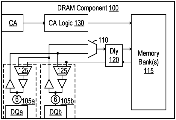
first and second memory components each having redundant and interconnected first and second memory-component data interfaces with respective first and second memory-component data ports;
a first memory-component substrate having a first signal trace extending from the first module data port through the first memory-component substrate, a second signal trace extending between the second module data port and the first memory-component data port of the first memory component, the second signal trace forming a first point-to-point connection from the second module data port to the first memory-component data port of the first memory component, and a third signal trace extending between the third module data port and the second memory-component data port of the first memory component; and
a second memory-component substrate having a fourth signal trace extending between the first signal trace of the first memory-component substrate and the first memory-component data port of the second memory component, the first and fourth signal traces forming a second point-to-point connection from the first module data port to the first memory-component data port of the second memory component, and a fifth signal trace extending between the third signal trace of the first memory-component substrate and the second memory-component data port of the second memory component.
|