US 11,955,161 B2
Command-triggered data clock distribution mode
Ian Shaeffer, Los Gatos, CA (US); Lei Luo, Chapel Hill, CA (US); and Liji Gopalakrishnan, Sunnyvale, CA (US)
Assigned to Rambus Inc., San Jose, CA (US)
Filed by Rambus Inc., San Jose, CA (US)
Filed on Jan. 30, 2023, as Appl. No. 18/103,386.
Application 18/103,386 is a continuation of application No. 17/341,048, filed on Jun. 7, 2021, granted, now 11,587,605.
Application 17/341,048 is a continuation of application No. 16/865,928, filed on May 4, 2020, granted, now 11,049,546, issued on Jun. 29, 2021.
Application 16/865,928 is a continuation of application No. 16/032,633, filed on Jul. 11, 2018, granted, now 10,665,289, issued on May 26, 2020.
Application 16/032,633 is a continuation of application No. 15/616,209, filed on Jun. 7, 2017, granted, now 10,026,466, issued on Jul. 17, 2018.
Application 15/616,209 is a continuation of application No. 15/242,423, filed on Aug. 19, 2016, granted, now 9,704,560, issued on Jul. 11, 2017.
Application 15/242,423 is a continuation of application No. 14/799,362, filed on Jul. 14, 2015, granted, now 9,430,027, issued on Aug. 30, 2016.
Application 14/799,362 is a continuation of application No. 13/980,368, granted, now 9,098,281, issued on Aug. 4, 2015, previously published as PCT/US2012/028289, filed on Mar. 8, 2012.
Claims priority of provisional application 61/451,023, filed on Mar. 9, 2011.
Prior Publication US 2023/0326513 A1, Oct. 12, 2023
Int. Cl. G06F 1/04 (2006.01); G06F 1/08 (2006.01); G06F 1/3234 (2019.01); G06F 1/3237 (2019.01); G11C 7/10 (2006.01); G11C 7/20 (2006.01); G11C 7/22 (2006.01); G11C 11/4072 (2006.01); G11C 11/4074 (2006.01); G11C 11/4076 (2006.01); G11C 11/408 (2006.01); G11C 11/4096 (2006.01)
CPC G11C 11/4076 (2013.01) [G06F 1/04 (2013.01); G06F 1/08 (2013.01); G06F 1/3234 (2013.01); G06F 1/3237 (2013.01); G11C 7/1072 (2013.01); G11C 7/20 (2013.01); G11C 7/22 (2013.01); G11C 11/4072 (2013.01); G11C 11/4074 (2013.01); G11C 11/4087 (2013.01); G11C 11/4096 (2013.01); Y02D 10/00 (2018.01); Y02D 30/50 (2020.08)] 21 Claims
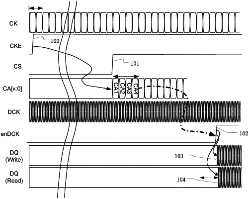
OG exemplary drawing
 
1. A method of controlling an integrated-circuit memory component (“memory IC”), the method comprising:
outputting a command/address clock signal and a data clock signal to the memory IC, the data clock signal having a frequency at least twice the frequency of the command/address clock signal; and
programming a first control value within a register within the memory IC to implement a configuration of the memory IC in which, after disabling distribution of the data clock signal within the memory IC to reduce power consumption, distribution of the data clock signal within the memory IC is re-enabled in response to receipt of a memory access command.