| CPC G11C 11/40615 (2013.01) [G11C 11/4085 (2013.01); H03M 13/1105 (2013.01); H03M 13/611 (2013.01); H01L 25/0657 (2013.01); H01L 2225/06541 (2013.01)] | 17 Claims |

|
1. A semiconductor memory device comprising:
a memory cell array including a plurality of memory cell rows, each including a plurality of memory cells;
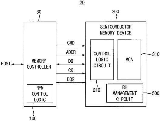
a row hammer management circuit configured to:
count a number of times of access associated with each of the plurality of memory cell rows in response to an active command from an external memory controller to store the counted values in each of the plurality of memory cell rows as count data,
determine a hammer address associated with at least one of the plurality of memory cell rows, which is intensively accessed more than a predetermined reference number of times, based on the counted values, and
in response to a first command applied after the active command, perform an internal read-update-write operation to read the count data from a target memory cell row from among the plurality of memory cell rows, to update the read count data, and to write the updated count data in the target memory cell row; and
a refresh control circuit configured to receive the hammer address and to perform a hammer refresh operation on one or more victim memory cell rows which are physically adjacent to a memory cell row corresponding to the hammer address,
wherein the semiconductor memory device is configured to perform a memory operation on the target memory cell row in response to a second command applied from the external memory controller after the active command, and
wherein the first command is applied from the external memory controller after a predetermined delay time from the second command.
|