| CPC G11C 11/2275 (2013.01) [G11C 11/223 (2013.01); G11C 11/2273 (2013.01); H01L 29/40111 (2019.08); H01L 29/78391 (2014.09); H01L 29/7881 (2013.01); H10B 51/30 (2023.02); H10B 53/30 (2023.02); G11C 11/2257 (2013.01)] | 5 Claims |

|
1. A method of reading memory cells of a memory array, comprising:
providing the memory array to have metal-ferroelectric-metal-insulator-semiconductor (MFMIS) transistors as the memory cells, with a first data state of the memory cells corresponding to a first polarization mode of ferroelectric material within the MFMIS transistors and a second data state of the memory cells corresponding to a second polarization mode of the ferroelectric material within the MFMIS transistors;
the individual MFMIS transistors comprising a gate and a pair of source/drain regions;
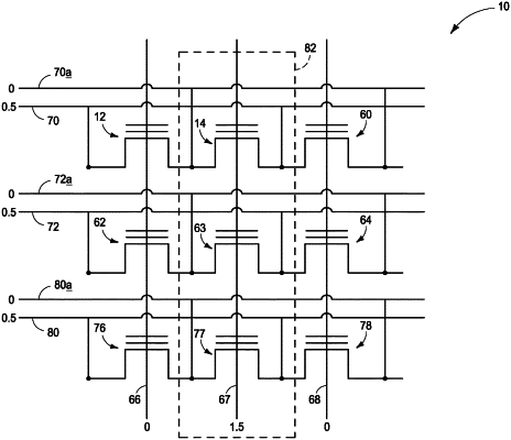
the memory array comprising rows and columns of the MFMIS transistors, each of the rows comprising a first transistor and a second transistor that share a common source/drain region and common contact extending upward from the common source/drain regions and between gates of the first and second transistors, a line of symmetry passing through the common source/drain region and common contact with the first transistor being a mirror image of the second transistor across the line of symmetry;
MFMIS transistors in a common row as one another having all of their gates electrically coupled to one another through a wordline;
MFMIS transistors in a common column as one another sharing a pair of digit lines; a first of the digit lines being connected to one source/drain region of each of the MFMIS transistors in said common column, and a second of the digit lines being connected to the other source/drain region of each of the MFMIS transistors in said common column;
identifying an active row comprising memory cells which are to be read; and
providing a voltage difference between the first and second digit lines for all of the memory cells within the active row while simultaneously providing a bias voltage along the wordline of the active row.
|