| CPC G11C 11/2273 (2013.01) [G11C 7/1039 (2013.01); G11C 11/2275 (2013.01); G11C 11/2297 (2013.01); H03K 19/01742 (2013.01); H03K 19/20 (2013.01)] | 44 Claims |

|
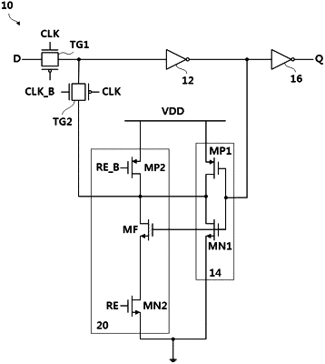
1. A nonvolatile memory device comprising:
a first inverter;
a second inverter cross-coupled to the first inverter; and
a nonvolatile memory circuit,
wherein the nonvolatile memory circuit includes a pull-up transistor, a pull-down transistor, and a ferroelectric field effect transistor (FeFET) of which a first electrode and a second electrode are respectively connected to the pull-up transistor and the pull-down transistor, and wherein when the ferroelectric field effect transistor is programmed to a low resistance state, an equivalent resistance of a current path including the pull-down transistor is smaller than an equivalent resistance of a current path including the pull-up transistor.
|