| CPC G09G 3/36 (2013.01) [G02F 1/136286 (2013.01); G09G 2300/0871 (2013.01); G09G 2330/02 (2013.01)] | 20 Claims |

|
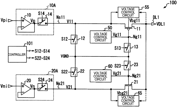
1. An output circuit, comprising:
a positive voltage signal supply circuit that supplies a positive voltage signal having a voltage higher than a reference power supply voltage to a first node or cuts off supply of the positive voltage signal to the first node;
a negative voltage signal supply circuit that supplies a negative voltage signal having a voltage lower than the reference power supply voltage to a second node or cuts off supply of the negative voltage signal to the second node;
a first output terminal;
a first switch which is composed of a first PMOS transistor switch in which a source is connected to the first node and a drain is connected to the first output terminal, and connects the first output terminal and the first node when the first switch is turned on and cuts off connection between the first output terminal and the first node when the first switch is turned off;
a second switch which is composed of a first NMOS transistor switch in which a source is connected to the second node and a drain is connected to the first output terminal, and connects the first output terminal and the second node when the second switch is turned on and cuts off connection between the first output terminal and the second node when the second switch is turned off;
a third switch that applies the reference power supply voltage to the first node when the third switch is turned on and stops application of the reference power supply voltage to the first node when the third switch is turned off;
a fourth switch that applies the reference power supply voltage to the second node when the fourth switch is turned on and stops application of the reference power supply voltage to the second node when the fourth switch is turned off;
a first voltage control circuit that is connected to a gate of the first switch and controls the first switch such that the first switch is brought into an on state;
a second voltage control circuit that is connected to a gate of the second switch and controls the second switch such that the second switch is brought into an on state;
a first control device that is connected to the gate of the first switch and controls the first switch such that the first switch is brought into an off state;
a second control device that is connected to the gate of the second switch and controls the second switch such that the second switch is brought into an off state;
a third voltage control circuit that sets a voltage of the source or the drain of the first PMOS transistor switch as a first voltage and controls whether a second voltage obtained by shifting the level of the first voltage to a high potential side is supplied to a back gate of the first PMOS transistor switch or the reference power supply voltage is supplied to the back gate of the first PMOS transistor switch; and
a fourth voltage control circuit that sets a voltage of the source or the drain of the first NMOS transistor switch as a third voltage and controls whether a fourth voltage obtained by shifting the level of the third voltage to a low potential side is supplied to a back gate of the first NMOS transistor switch or the reference power supply voltage is supplied to the back gate of the first NMOS transistor switch.
|