US 11,955,092 B2
Display device, and method of sensing a driving characteristic
Jeonkyoo Kim, Seoul (KR); Soo Yeon Lee, Seoul (KR); Manseung Cho, Seoul (KR); Kyeong Soo Kang, Seongnam-si (KR); Junhee Moon, Suwon-si (KR); Bonghyun You, Seoul (KR); and Jin Kyu Lee, Seoul (KR)
Assigned to SAMSUNG DISPLAY CO., LTD., Gyeonggi-Do (KR); and SEOUL NATIONAL UNIVERSITY R&DB FOUNDATION, Seoul (KR)
Filed by Samsung Display Co., Ltd., Yongin-si (KR); and SEOUL NATIONAL UNIVERSITY R&DB FOUNDATION, Seoul (KR)
Filed on Apr. 15, 2023, as Appl. No. 18/135,152.
Application 18/135,152 is a continuation of application No. 17/874,680, filed on Jul. 27, 2022, granted, now 11,631,374.
Application 17/874,680 is a continuation of application No. 17/346,655, filed on Jun. 14, 2021, granted, now 11,430,394.
Claims priority of application No. 10-2020-0085356 (KR), filed on Jul. 10, 2020.
Prior Publication US 2023/0252947 A1, Aug. 10, 2023
This patent is subject to a terminal disclaimer.
Int. Cl. G09G 3/3291 (2016.01); G09G 3/3233 (2016.01); G09G 3/3266 (2016.01)
CPC G09G 3/3291 (2013.01) [G09G 3/3266 (2013.01); G09G 2310/08 (2013.01)] 26 Claims
OG exemplary drawing
 
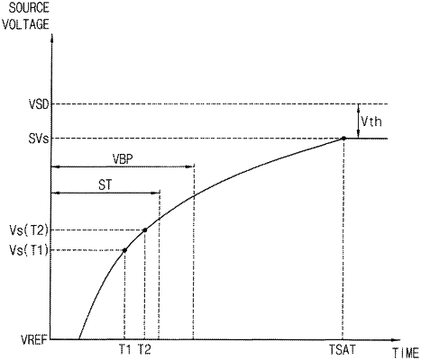
1. A display driver for driving a display panel, the display driver comprising: a data driver coupled to a data line of the display panel; a sensing circuit coupled to a sensing line of the display panel; and a controller which controls the data driver and the sensing circuit, wherein a vertical blank period of a frame period includes a sensing time, wherein the sensing circuit measures a first source voltage of a driving transistor of a pixel included in the display panel at a first time point of the sensing time, and measures a second source voltage of the driving transistor at a second time point of the sensing time, and wherein the controller corrects input image data for the pixel based on a predicted saturated source voltage of the driving transistor corresponding to the first and second source voltages.