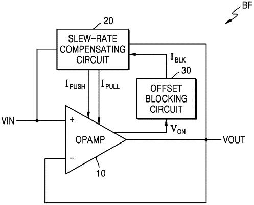
| CPC G09G 3/3275 (2013.01) [H03F 3/45269 (2013.01); G09G 2310/0243 (2013.01); G09G 2310/0291 (2013.01); G09G 2320/0204 (2013.01); G09G 2330/02 (2013.01)] | 20 Claims |

|
1. A buffer circuit comprising:
an operational amplifier configured to amplify an input voltage to generate an output voltage;
a slew-rate compensating circuit including a boosting transistor, the slew-rate compensating circuit configured to generate a compensation current based on a difference between a voltage level of the input voltage and a voltage level of the output voltage and provide the compensation current to the operational amplifier through the boosting transistor; and
an offset blocking circuit configured to turn off the boosting transistor in response to the difference between the voltage level of the input voltage and the voltage level of the output voltage being less than a reference voltage level by providing a blocking current to a gate of the boosting transistor.
|