| CPC G09G 3/3275 (2013.01) [H10K 59/131 (2023.02); G09G 2310/061 (2013.01)] | 11 Claims |

|
1. A display substrate, comprising:
a base substrate;
a first pixel and a second pixel disposed on the base substrate, wherein the first pixel and the second pixel are arranged along a first direction and are adjacent, and both the first pixel and the second pixel comprise a pixel circuit and a light emitting element, the pixel circuit comprising a drive transistor, a first reset transistor, and a second reset transistor; wherein
the first reset transistor is coupled to a first reset control line, a first reset signal line, and a gate of the drive transistor, and the first reset transistor is configured to, in response to a first reset control signal provided by the first reset control line, transmit a first reset signal provided by the first reset signal line to the gate of the drive transistor to reset the gate of the drive transistor; and
the second reset transistor is coupled to a second reset control line, a second reset signal line, and a first electrode of the light emitting element, and the second reset transistor is configured to, in response to a second reset control signal provided by the second reset control line, transmit a second reset signal provided by the second reset signal line to the first electrode of the light emitting element to reset the first electrode of the light emitting element;
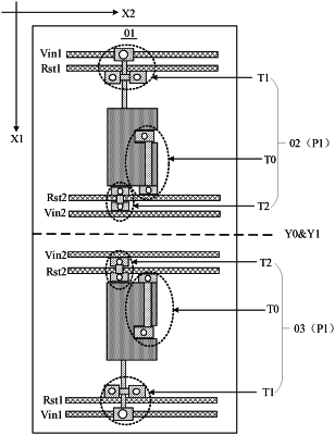
wherein the first reset signal line comprises a first portion extending along a second direction, and the first reset transistors, the second reset transistors, and the drive transistors in the first pixel and in the second pixel are arranged symmetrically along a symmetry axis of the first portion respectively, the second direction being a row direction, and the second direction being intersected with the first direction;
the second reset signal line comprises a second portion extending along the second direction; the first reset transistors, the second reset transistors, and the drive transistors in the first pixel and in the second pixel are arranged symmetrically along a symmetry axis of the second portion respectively;
the first reset control line extends along the second direction, and the first reset control line coupled to the pixel circuit in the first pixel and the first reset control line coupled to the pixel circuit in the second pixel are arranged symmetrically along the symmetry axis of the first portion;
the second reset control line extends along the second direction, and the second reset control line coupled to the pixel circuit in the first pixel and the second reset control line coupled to the pixel circuit in the second pixel are arranged symmetrically along the symmetry axis of the second portion; and
the symmetry axis of the first portion is overlapped with the symmetry axis the second portion.
|