| CPC G09G 3/3266 (2013.01) [G09G 3/3233 (2013.01); G09G 2300/0842 (2013.01); G09G 2310/0297 (2013.01); G09G 2310/08 (2013.01); G09G 2320/0247 (2013.01); G09G 2320/043 (2013.01); G09G 2320/0673 (2013.01); G09G 2330/021 (2013.01)] | 23 Claims |

|
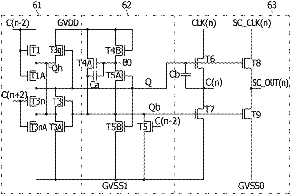
1. An inverter circuit comprising:
a first transistor connected between a high potential voltage line and a first node;
a second transistor having a gate connected to the first node and turned on according to a voltage of the first node to charge a second control node to a high potential voltage applied to the high potential voltage line;
a third transistor having a gate connected to a first control node, a first electrode connected to the first node, and a second electrode directly connected to the second control node; and
a fourth transistor having a gate connected to the first control node, a first electrode directly connected to the second control node, and a second electrode connected to a low potential voltage line,
wherein the third transistor and the fourth transistor are turned on according to a voltage of the first control node to discharge the second control node to a low potential voltage applied to the low potential voltage line,
wherein the third transistor and the fourth transistor are connected in series between the first node and the low potential voltage line, and
wherein the first control node is an output node of the inverter circuit.
|