| CPC G09G 3/3258 (2013.01) [G09G 3/3266 (2013.01); G09G 3/3291 (2013.01); G09G 2300/0842 (2013.01); G09G 2330/021 (2013.01)] | 20 Claims |

|
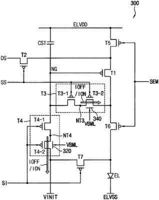
1. A pixel of an organic light emitting diode display device, the pixel comprising:
a storage capacitor comprising a first electrode connected to a line of a first power supply voltage, and a second electrode connected to a gate node;
a first transistor comprising a gate electrode connected to the gate node;
a second transistor configured to transfer a data signal to a source of the first transistor in response to a scan signal;
a third transistor configured to diode-connect the first transistor in response to the scan signal, the third transistor comprising first and second sub-transistors serially connected between the gate node and a drain of the first transistor, the first and second sub-transistors comprising first and second active regions spaced from each other in a plan view, first and second gate electrodes overlapping with the first and second active regions, respectively, and a node of the third transistor between the first and second active regions of the first and second sub-transistors;
a fourth transistor configured to transfer an initialization voltage to the gate node in response to an initialization signal, the fourth transistor comprising third and fourth sub-transistors serially connected between the gate node and a line of the initialization voltage, the third and fourth sub-transistors comprising third and fourth active regions spaced from each other in a plan view, third and fourth gate electrodes overlapping with the third and fourth active regions, respectively, and a node of the fourth transistor between the third and fourth active regions of the third and fourth sub-transistors; and
an organic light emitting diode comprising an anode, and a cathode connected to a line of a second power supply voltage,
wherein at least one of the second sub-transistor or the fourth sub-transistor comprises a bottom electrode to decrease a voltage of at least one of the node of the third transistor or the node of the fourth transistor in response to a bottom electrode voltage,
wherein, in a plan view, the bottom electrode overlaps with at least one of the second gate electrode or the fourth gate electrode, while being spaced from the first gate electrode and the third gate electrode,
wherein at least one of the second gate electrode or the fourth gate electrode is disposed over a corresponding one of the second active region and the fourth active region, and the bottom electrode is disposed under the corresponding one of the second active region and the fourth active region,
wherein, in a plan view, an end of the bottom electrode overlaps with a space defined between the first and second gate electrodes or between the third and fourth gate electrodes, and
wherein the bottom electrode is configured to receive a bottom electrode voltage during a masking period in which a display panel of the organic light emitting diode display device is not driven such that the display panel displays an image based on previously stored data signals of a previous frame period.
|