| CPC G09G 3/3233 (2013.01) [G09G 2300/043 (2013.01); G09G 2300/0819 (2013.01); G09G 2300/0842 (2013.01); G09G 2300/0861 (2013.01); G09G 2310/08 (2013.01); G09G 2320/0233 (2013.01)] | 19 Claims |

|
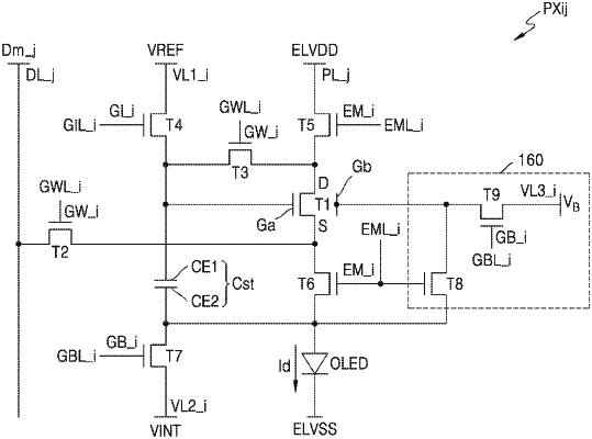
1. A pixel comprising:
a display element configured to emit light for an emission period, and including an anode and a cathode;
a driving transistor configured to control an amount of a driving current flowing through the display element, wherein the driving transistor includes a first gate and a second gate;
a storage capacitor electrically connected to the first gate of the driving transistor;
a scan transistor configured to be turned on for a data-write period and to transfer a data voltage to the driving transistor; and
a gate control circuit configured to electrically connect the second gate of the driving transistor to the anode of the display element for the emission period, and configured to apply a bias voltage to the second gate of the driving transistor for the data-write period,
wherein a voltage between the second gate and a source of the driving transistor is at a first level for the data-write period, and is at a second level for the emission period, wherein the second level is higher than the first level.
|