| CPC G09G 3/3233 (2013.01) [H10K 59/131 (2023.02); G09G 2300/0426 (2013.01); G09G 2320/0233 (2013.01)] | 18 Claims |

|
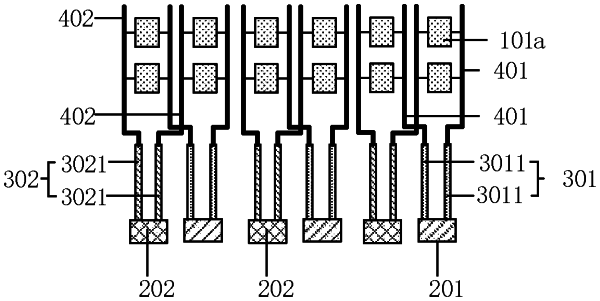
1. An array substrate having a display area and a non-display area, the non-display area including a first bonding region and a fan-out region located between the display area and the first bonding region, the array substrate comprising:
a plurality of pixel columns disposed in the display area, each of the plurality of pixel columns including a plurality of light-emitting units that are arranged in a second direction, the second direction being perpendicular to a direction in which an edge of the display area proximate to the first bonding region extends;
at least three first power supply input terminals disposed in the first bonding region, each first power supply input terminal being connected to multiple pixel columns of the plurality of pixel columns, so as to provide a first power supply signal to the multiple pixel columns; and
at least three first fan-out structures located in the fan-out region, each first power supply input terminal being electrically connected to the multiple pixel columns of the plurality of pixel columns through one first fan-out structure, and resistances of the first fan-out structures being equal, wherein
each first power supply input terminal refers to a first power supply input pad; and
each first fan-out structure of the at least three first fan-out structures includes a plurality of first conductive units; the plurality of first conductive units are parallel to each other, and each independently electrically connected to a corresponding one of at least three first power supply input terminals; and each of the plurality of first conductive units is electrically connected to at least one of the plurality of pixel columns.
|