| CPC G09G 3/3225 (2013.01) [G09G 2310/0297 (2013.01); G09G 2310/08 (2013.01); G09G 2320/0257 (2013.01)] | 13 Claims |

|
1. A pixel circuit, comprising:
a drive transistor comprising a gate electrode, a first electrode and a second electrode;
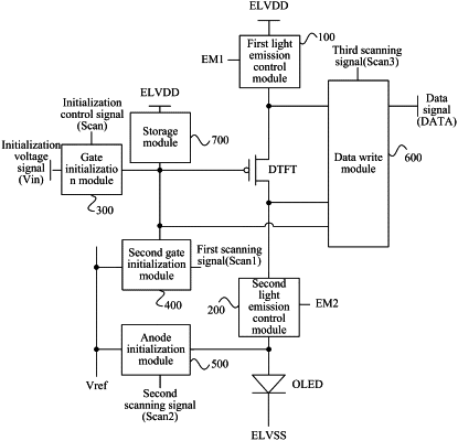
a first light emission control module comprising a first transistor, a gate electrode of the first transistor electrically connected with a first light emission control signal, a first electrode of the first transistor is electrically connected with a first power signal, and a second electrode of the first transistor is electrically connected to the first electrode of the drive transistor;
a second light emission control module comprising a second transistor, a gate electrode of the second transistor is electrically connected with a second light emission control signal, a first electrode of the second transistor is electrically connected to the second electrode of the drive transistor, and a second electrode of the second transistor is electrically connected to an anode of a light emission device;
a gate initialization module comprising a third transistor, a gate electrode of the third transistor is electrically connected with an initialization control signal, a first electrode of the third transistor is electrically connected with an initialization voltage signal, and a second electrode of the third transistor is electrically connected to the gate electrode the drive transistor;
a second gate initialization module comprising a fourth transistor, a gate electrode of the fourth transistor is electrically connected with a first scanning signal, a first electrode of the fourth transistor is electrically connected to the second electrode of the drive transistor, and a second electrode of the fourth transistor is electrically connected to the gate electrode of the drive transistor;
an anode initialization module comprising a fifth transistor, a first electrode of the fifth transistor is electrically connected with a reference voltage signal and a second electrode of the fifth transistor is electrically connected to the second electrode of the drive transistor; and
a data write module comprising a sixth transistor, a gate electrode of the sixth transistor is electrically connected with a third scanning signal, a first electrode of the sixth transistor is electrically connected with a data signal, and a second electrode of the sixth transistor is electrically connected to the first electrode of the drive transistor;
wherein the fourth transistor is multiplexed as a transistor in the data write module such that the pixel circuit is a 7T1C circuit provided with at most seven transistors, including the drive transistor.
|