| CPC G09G 3/32 (2013.01) [G09G 3/03 (2020.08); G09G 3/3266 (2013.01); G09G 2300/0842 (2013.01); G09G 2310/0267 (2013.01); G09G 2310/061 (2013.01)] | 18 Claims |

|
1. A display substrate, comprising a base substrate, wherein the base substrate comprises a display region and a peripheral region on at least one side of the display region,
wherein the display region comprises a plurality of rows and a plurality of columns of pixel units arranged in an array, a plurality of gate scanning signal lines respectively connected to the plurality of rows of pixel units, and a plurality of connecting lines in different layers from the plurality of gate scanning signal lines;
the peripheral region comprises a first peripheral sub-region and a second peripheral sub-region, the display region comprises a first display sub-region corresponding to the first peripheral sub-region and a second display sub-region corresponding to the second peripheral sub-region, and the second display sub-region is different from the first display sub-region;
the second peripheral sub-region comprises a first gate driving circuit, and the first gate driving circuit is configured to be connected to a plurality of gate scanning signal lines in the first display sub-region through the plurality of connecting lines in the display region, to respectively providing gate scanning signals to a plurality of rows of pixel units in the first display sub-region; and
the first peripheral sub-region does not comprise the first gate driving circuit;
wherein the second peripheral sub-region further comprises a second gate driving circuit, and the second gate driving circuit is configured to be connected to a plurality of gate scanning signal lines in the second display sub-region, to respectively providing the gate scanning signal to a plurality of rows of pixel units in the second display sub-region; and
the first peripheral sub-region does not comprise the second gate driving circuit;
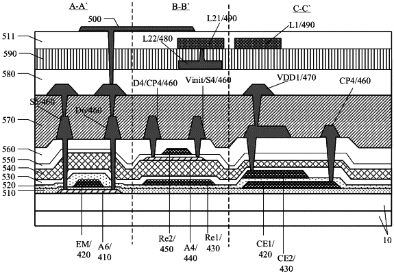
wherein each of the plurality of connecting lines comprises a first line extending in a first direction and a second line extending in a second direction, the first direction intersects the second direction; and
the first gate driving circuit is connected to the first line through the second line, and the first line is connected to a corresponding gate scanning signal line in the first display sub-region through a via hole passing through an insulating layer, to providing the gate scanning signal to the corresponding gate scanning signal line.
|