| CPC G06K 7/10316 (2013.01) [G06K 19/0723 (2013.01); H01Q 7/00 (2013.01); H05K 1/0243 (2013.01); H05K 1/165 (2013.01); H05K 2201/10098 (2013.01)] | 18 Claims |

|
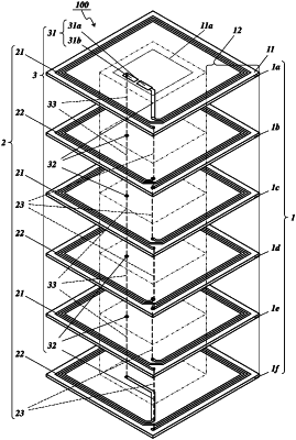
1. An RFID tag substrate comprising:
an insulating substrate that has a mounting region in which a semiconductor device is disposed, the mounting region being included in a first surface of the insulating substrate; and
a coil that is positioned at an outer edge portion of the insulating substrate,
wherein the coil includes a plurality of first coil conductors and a plurality of second coil conductors each having a same line width that are wound such that the first coil conductors and the second coil conductors each have the same number of turns and such that a direction in which the first coil conductors are wound and a direction in which the second coil conductors are wound are opposite to each other, and
wherein the first coil conductors and the second coil conductors are alternately arranged in a thickness direction of the insulating substrate and connected in series to one another.
|