US 11,953,826 B2
Lined photobucket structure for back end of line (BEOL) interconnect formation
James M. Blackwell, Portland, OR (US); Robert L. Bristol, Portland, OR (US); Marie Krysak, Portland, OR (US); Florian Gstrein, Portland, OR (US); Eungnak Han, Portland, OR (US); Kevin L. Lin, Beaverton, OR (US); Rami Hourani, Portland, OR (US); and Shane M. Harlson, Beaverton, OR (US)
Assigned to Intel Corporation, Santa Clara, CA (US)
Filed by Intel Corporation, Santa Clara, CA (US)
Filed on Sep. 1, 2021, as Appl. No. 17/464,393.
Application 17/464,393 is a continuation of application No. 16/097,960, granted, now 11,137,681, previously published as PCT/US2016/040876, filed on Jul. 1, 2016.
Prior Publication US 2021/0397084 A1, Dec. 23, 2021
Int. Cl. G03F 7/00 (2006.01); G03F 7/40 (2006.01); H01L 21/027 (2006.01); H01L 21/768 (2006.01)
CPC G03F 7/0035 (2013.01) [G03F 7/0002 (2013.01); G03F 7/40 (2013.01); H01L 21/027 (2013.01); H01L 21/0274 (2013.01); H01L 21/768 (2013.01); H01L 21/76802 (2013.01)] 20 Claims
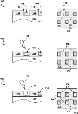
OG exemplary drawing
 
1. An integrated circuit structure, comprising:
a plurality of recesses in a layer disposed on an interlayer dielectric material layer;
for each recess of the plurality of recesses:
a respective liner structure in the recess; and
a respective photobucket in the recess, wherein the photobucket is surrounded by the liner structure in the recess.