| CPC G02F 1/136286 (2013.01) [G02F 1/136209 (2013.01)] | 9 Claims |

|
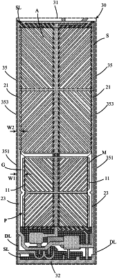
1. A pixel unit of a display panel, disposed to correspond to an aperture region formed by two scan lines perpendicularly intersecting two data lines, and the pixel unit comprising:
a light shielding matrix element disposed above the two data lines and comprising two light shielding strips parallel to the two data lines; and
a pixel electrode comprising:
a main pixel electrode portion, wherein the main pixel electrode portion comprises two side edges near the two data lines respectively; and
a sub-pixel electrode portion comprises two side edges near the two data lines respectively and two connection lines extending from the two side edges respectively;
wherein each of the light shielding strips shields a corresponding one of the data lines and a corresponding one of the connection lines, and the light shielding strips overlap the two side edges of the main pixel electrode portion respectively and overlap the two side edges of the sub-pixel electrode portion respectively;
wherein the two connection lines of the sub-pixel electrode portion extending toward the main pixel electrode portion, and each of the connection line at least partially overlap a corresponding one of the data lines;
wherein a gap is formed between each of the side edges of the main pixel electrode portion and a corresponding one of the connection lines; and
wherein each of the light shielding strips comprises:
a first light shielding section shielding a section of one of the data lines near the main pixel electrode portion and one of the connection lines, and overlapping one of the side edges of the main pixel electrode portion; and
a second light shielding section connected to the first light shielding section, shielding a section of one of the data lines near the sub-pixel electrode portion, and overlapping one of the side edges of the sub-pixel electrode portion.
|