|
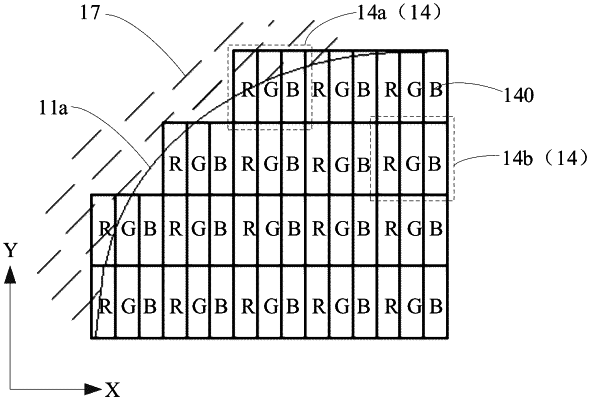
1. An irregularly-shaped display panel, comprising a pixel unit and a shielding layer, wherein a plurality of pixel units are provided and are arranged in an array; each of the plurality of pixel units comprises a plurality of sub-pixels, an opening region of each of the plurality of sub-pixels comprises a pixel electrode and a common electrode which is opposite to the pixel electrode and is insulated from the pixel electrode, and a pixel voltage difference is formed between the common electrode and the pixel electrode; wherein some of the plurality of pixel units are shielded by the shielding layer to form irregularly-shaped pixel units, and each of the irregularly-shaped pixel units at least comprises a first irregularly-shaped pixel unit; in the first irregularly-shaped pixel unit, the area of an opening region of at least one sub-pixel shielded by the shielding layer is greater than 0 and less than the area of an opening region of at least one sub-pixel, and the areas of opening regions of the remaining sub-pixels shielded by the shielding layer are greater than or equal to 0 and less than the area of an opening region of the remaining sub-pixels; and wherein in the first irregularly-shaped pixel unit, the areas of opening regions of at least two sub-pixels shielded by the shielding layer are different, and the sub-pixel having a larger area of an opening region shielded by the shielding layer has a larger pixel voltage difference.
|
