| CPC G02F 1/133512 (2013.01) [G02F 1/13338 (2013.01); G02F 1/134345 (2021.01); G02F 1/136286 (2013.01); G02F 1/1368 (2013.01); G06V 40/1318 (2022.01); H01L 27/124 (2013.01); G02F 1/13439 (2013.01)] | 13 Claims |

|
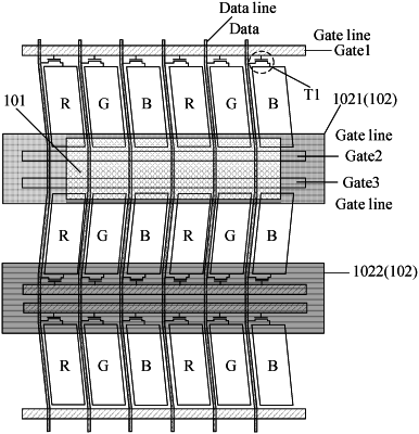
1. A display substrate, comprising
a base substrate;
a plurality of sub-pixels on the base substrate, every two rows of sub-pixels constituting a pixel group;
a plurality of first gate lines at first row gaps between adjacent pixel groups, two first gate lines being arranged at each first row gap; and
a plurality of photosensors; wherein orthographic projections of each row of photosensors on the base substrate completely cover a second row gap in the pixel group, and partially overlap with orthographic projections of the sub-pixels;
wherein each of the sub-pixels comprises:
a first transistor between a layer where the plurality of photosensors are located and the base substrate; and
a planar common electrode, an insulating layer and a slit pixel electrode sequentially located on a side, facing away from a layer where the first transistors are located, of the layer where the plurality of photosensors are located;
wherein in one first row gap, one row of the first transistors is electrically connected to one first gate line at the first row gap, and another row of the first transistors is electrically connected to another first gate line at the first row gap; and
the slit pixel electrodes are electrically connected to the first transistors.
|