| CPC G02F 1/01708 (2013.01) | 20 Claims |

|
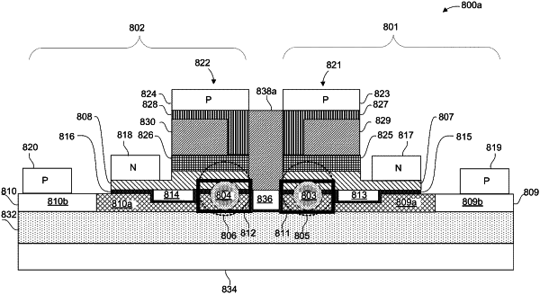
1. A hybrid III-V/silicon device comprising:
a first silicon layer disposed over a buried oxide (BOX) layer, wherein the first silicon layer includes:
a first doped region having a first trench,
a second doped region having a second trench,
a first gap region disposed between the first doped region and the second doped region;
a first oxide layer disposed over the first doped region and the second doped region;
a first mesa disposed on the first doped region of the first silicon layer, wherein the first mesa includes:
a first Group III-V layer disposed over the first oxide layer;
a first optically active region disposed over the first Group III-V layer; and
a second Group III-V layer disposed over the optically active region; and
a second mesa disposed on the second doped region of the first silicon layer, wherein the second mesa includes:
a third Group III-V layer disposed over the first oxide layer;
a second optically active region disposed over the third Group III-V layer; and
a fourth Group III-V layer disposed over the second optically active region.
|