| CPC G01R 31/2642 (2013.01) [G01R 31/2621 (2013.01); G01R 31/275 (2013.01); G01R 31/2884 (2013.01); G11C 29/022 (2013.01); H01L 22/34 (2013.01); H01L 2924/00 (2013.01); H01L 2924/0002 (2013.01)] | 8 Claims |

|
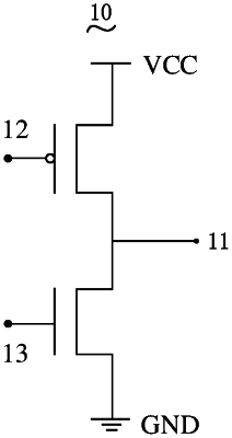
1. A test method for tolerance against a hot carrier effect, applied to an input/output (I/O) circuit of a memory, the I/O circuit having an output terminal, and the I/O circuit comprising a p-channel metal-oxide semiconductor (PMOS) transistor and an n-channel metal-oxide semiconductor (NMOS) transistor, the output terminal being respectively connected to a drain of the PMOS transistor and a drain of the NMOS transistor, a source of the PMOS transistor being connected to an operating power supply, and a source of the NMOS transistor being grounded; and the test method for tolerance against the hot carrier effect comprising:
controlling the output terminal to alternately output a first level and a second level, comprising: at a previous moment, the PMOS transistor being controlled to be turned on and the NMOS transistor being controlled to be turned off, to enable the output terminal to output the first level; and at a latter moment, the PMOS transistor being controlled to be turned off and the NMOS transistor being controlled to be turned on to enable the output terminal to output the second level; wherein the first level is higher than the second level;
obtaining degradation rates of output performance parameters of the I/O circuit according to the first level and the second level, wherein the degradation rates comprise at least one of a level maximum and minimum degradation rate or a level conversion rate degradation rate, and the level conversion rate degradation rate comprises a level rising edge conversion rate degradation rate and a level falling edge conversion rate degradation rate; and
obtaining a first tolerance against the hot carrier effect of the PMOS transistor and a second tolerance against the hot carrier effect of the NMOS transistor, based on the degradation rates.
|