| CPC G01J 1/44 (2013.01) [G01J 1/0411 (2013.01); G01J 1/0437 (2013.01); H01L 27/14623 (2013.01); H01L 27/14627 (2013.01); G01J 2001/446 (2013.01); G01J 2001/4473 (2013.01); G06V 40/1318 (2022.01)] | 18 Claims |

|
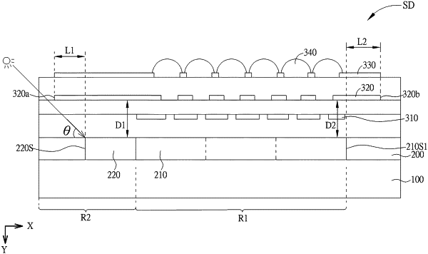
1. An optical sensing device, comprising:
a sensing pixel comprising a sensing circuit and a sensing element electrically connected to the sensing circuit;
a driving circuit electrically connected to the sensing circuit;
a first light shielding layer comprising at least one first opening corresponding to the sensing element;
a second light shielding layer comprising at least one second opening overlapped with the at least one first opening in a top-view direction of the optical sensing device, wherein the second light shielding layer is overlapped with the driving circuit in the top-view direction; and
a third light shielding layer comprising at least one third opening overlapped with the at least one first opening in the top-view direction,
wherein an edge of the second light shielding layer corresponds to a peripheral region of the optical sensing device, and a horizontal distance between the edge of the second light shielding layer and the sensing pixel is greater than a horizontal distance between the edge of the second light shielding layer and the driving circuit,
wherein the second light shielding layer is overlapped with the third light shielding layer in the peripheral region, and a boundary between the peripheral region and a sensing region of the optical sensing device is at an outer side of an edge of the first light shielding layer,
wherein another edge of the second light shielding layer adjacent to the sensing pixel extends outward from the sensing pixel by a second extension distance, a vertical distance between the second light shielding layer and the sensing pixel in the top-view direction is defined as a second spacing, and the second extension distance is greater than or equal to the second spacing.
|