| CPC G01B 15/02 (2013.01) [G01N 23/2251 (2013.01); H01J 37/1478 (2013.01); G01N 2223/401 (2013.01); G01N 2223/6116 (2013.01); G01N 2223/6462 (2013.01); H01J 2237/1506 (2013.01)] | 20 Claims |

|
1. A system of examination of a semiconductor specimen, the system comprising a processor and memory circuitry (PMC) configured to:
obtain:
a first image of an area of a given semiconductor specimen acquired by an electron beam examination tool at a first illumination angle, wherein the first image is associated with a first grey level intensity profile, and
a second image of the area acquired by the electron beam examination tool at a second illumination angle, different from the first illumination angle, wherein the second image is associated with a second grey level intensity profile; and
use the first grey level intensity profile and the second grey level intensity profile to solve an optimization problem enabling determining a plurality of height values informative of a height profile of the given semiconductor specimen in the area,
wherein solving said optimization problem comprises:
determining at least one given height value of the plurality of height values such that, for a first location in the first image with a first grey level intensity, and a second location to be determined in the second image with a second grey level intensity and depending on said given height value, (1) and (2) are met:
(1) the second grey level intensity, or data informative thereof, matches the first grey level intensity, or data informative thereof, according to an optimization criterion, and
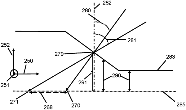
(2) a relationship between the second location and the first location complies with a model which models, for a given point of the specimen located at a given location in the first image, an expected position of this given point in the second image, as a function of at least the first illumination angle, the second illumination angle and the height profile of the specimen; and
wherein solving the optimization problem comprises using a corrective term in the optimization problem which takes into account dependency of grey level intensity with respect to illumination angle, wherein all images of the area of the given semiconductor specimen acquired by the electron beam examination tool and used in solving the optimization problem to determine a plurality of different height values informative of the height profile of the given semiconductor specimen have been acquired by the electron beam examination tool using a same given focal plane, said all images including the first image and the second image.
|