| CPC G01B 11/2522 (2013.01) [G06T 7/0004 (2013.01); H04N 23/56 (2023.01); G06T 2207/30148 (2013.01)] | 6 Claims |

|
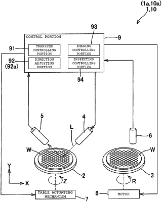
1. An imaging device for imaging a substrate that includes bumps that are on a substrate surface and are arranged at positions that correspond to points of intersection of a grid, the imaging device comprising:
a light emitting portion that emits light in a direction that is inclined relative to the substrate surface;
an imaging portion that images the substrate surface onto which the light is emitted; and
a direction adjusting portion that adjusts an arrangement relation between the direction in which the light is emitted and an orientation of the substrate to allow a diagonal direction that passes through diagonal positions of the grid to substantially correspond to the direction in which the light is emitted, in a plan view,
wherein the imaging portion images the substrate while the diagonal direction substantially corresponds to the direction in which the light is emitted, in a plan view.
|