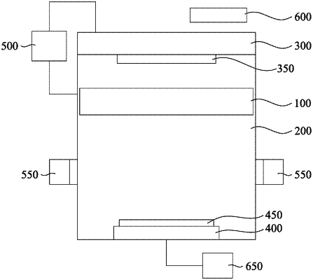
| CPC C23C 14/354 (2013.01) [C23C 14/50 (2013.01); H01J 37/3441 (2013.01); H01J 37/3447 (2013.01)] | 20 Claims |

|
1. A physical vapor deposition (PVD) system, comprising:
a pedestal configured to hold a semiconductor wafer;
a cover plate configured to hold a target; and
a collimator between the pedestal and the cover plate, wherein the collimator comprises a plurality of passages configured to pass source material travelling from the cover plate toward the pedestal at an angle less than a threshold angle with respect to a line perpendicular to a surface of the pedestal facing the cover plate, wherein the collimator is configured to block source material travelling from the cover plate toward the pedestal at an angle greater than the threshold angle, wherein a first passage of the plurality of passages has a first passage length, wherein a second passage of the plurality of passages has a second passage length, and wherein the first passage length is less than the second passage length; and, wherein
a central portion of the collimator has a cross sectional shape defined by a rectangle from which a trapezoid has been subtracted to form a cutout, wherein the first passage is in the central portion and the second passage is outside the central portion.
|