| CPC C23C 14/351 (2013.01) [C23C 14/345 (2013.01); C23C 14/3485 (2013.01); H01J 37/3405 (2013.01); H01J 37/3458 (2013.01); H01J 37/3467 (2013.01)] | 5 Claims |

|
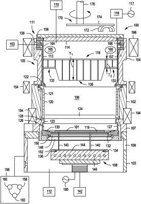
1. A physical vapor deposition processing chamber, comprising:
a chamber body defining a processing volume;
a substrate support disposed within the processing volume and comprising a substrate support surface configured to support a substrate, wherein an RF power source is configured to provide an AC bias power of greater than zero up to about 1000 W to the substrate support;
a power supply configured to energize a target when disposed in the processing volume for sputtering material toward the substrate;
a collimator;
a first electromagnet disposed above the collimator;
a second electromagnet that is disposed below the first electromagnet;
a third electromagnet between the first electromagnet and the second electromagnet;
the second electromagnet and third electromagnet operably coupled to the chamber body and positioned to form electromagnetic field lines through a sheath above the substrate during sputtering for directing sputtered material toward the substrate; and
a controller operably coupled to the physical vapor deposition processing chamber and programmed to control the second electromagnet and the third electromagnet based on a recipe comprising a pulsing schedule to the second electromagnet and the third electromagnet to supply a current to the third electromagnet different from a current to the second electromagnet, wherein the current to the second electromagnet is about −25 A to about 25 A with a frequency of a pulse being about 0 Hz to about 2000 Hz, and the current to the third electromagnet being about −25 A to about 25 A with a frequency of a pulse being about 0 Hz to about 2000 Hz, resulting in agitation of ions at a surface of the substrate to widen angular distribution of incident ions as ions approach the sheath and to control the ions relative to a feature on the substrate to improve overhang and increase coverage of sputtered material from the target on a sidewall of the feature relative to a bottom of the feature, wherein a ratio of sputtered material deposited on the sidewall of the feature and the bottom of the feature without the AC bias power is greater than a ratio of sputtered material deposited on the sidewall and the bottom of the feature on the substrate with the AC bias power.
|