| CPC B23K 26/361 (2015.10) [B23K 26/035 (2015.10); B23K 26/062 (2015.10); H01L 21/02021 (2013.01); H01L 22/10 (2013.01)] | 20 Claims |

|
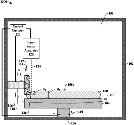
1. A method comprising:
aligning a wafer structure over a wafer chuck within a processing chamber;
rotating the wafer chuck to spin the wafer structure within the processing chamber;
trimming and removing an edge portion of the wafer structure using a blade to define a new sidewall of the wafer structure;
applying a confocal laser beam to a top surface of the wafer structure at an analysis area of the wafer structure arranged directly between the blade and a center of the wafer structure, wherein the analysis area is arranged closer to the blade than the center of the wafer structure;
measuring a parameter of the analysis area at the same time as the trimming by using a laser sensor apparatus that applies the confocal laser beam; and
performing a damage prevention process using control circuitry coupled to the laser sensor apparatus, the wafer chuck, and/or the blade if the parameter of the analysis area deviates from a predetermined threshold value by at least a predetermined shift value.
|