| CPC H10N 52/80 (2023.02) [C01B 32/194 (2017.08); G01R 33/07 (2013.01); H10N 52/01 (2023.02); B82Y 15/00 (2013.01); B82Y 40/00 (2013.01); C01B 2204/22 (2013.01); H10N 52/101 (2023.02)] | 10 Claims |
|
1. A method for connecting an electrical contact to a nanomaterial of at least one dimension supported by a substrate, the method comprising:
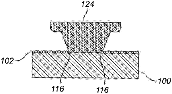
providing a substrate supporting a nanomaterial of at least one dimension and at least one layer of soluble lithography resist applied on the nanomaterial, wherein an opening in the at least one layer of resist exposes a portion of the nanomaterial, wherein, in the opening, an upper portion of the at least one layer of resist extends beyond a lower portion of the at least one layer of resist, thereby forming an overhang portion,
removing at least a portion of the exposed portion of the nanomaterial, thereby exposing the underlying substrate and an edge of the nanomaterial,
depositing a metal on at least the edge of the nanomaterial and the exposed substrate, the metal forming an electrical contact with the nanomaterial,
removing at least a portion of the soluble lithography resist from the nanomaterial such that at least a portion of the nanomaterial is exposed.
|